Negative electronic resistor SAN is a representative of the line of electronic resistors based on styrene copolymers. It is stable, easy to process and compatible with all CMOS processes. The resolution of 50 nm in pairs of lines has been reached.
Table 1 shows the parameters of the SAN resistor and the reagents for its processing.
| Parameters | Parameter value | Designation |
| Concentration, % | 2 | SAN-2 |
| Concentration, % | 3 | SAN-3 |
| Concentration, % | 5 | SAN-5 |
| Diluent | SAN-T | |
| Layer thickness, nm | ||
| Showman | SAN-D | |
| Rinse aid | SAN-R | |
| Removalist | Unexposed layer washing | SAN-S |
| Removalist | O2 is plasma. | |
Adhesion promoter | GMDS | 20% toluene solution |
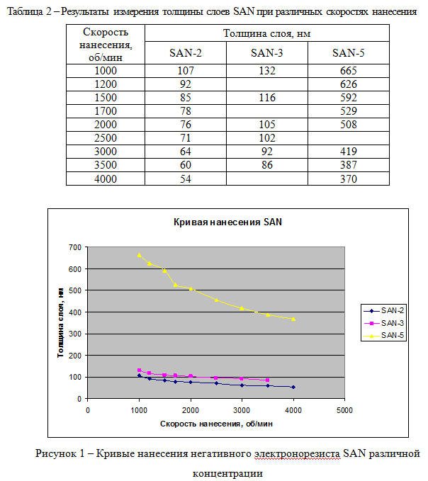
The dependence of the layer thickness on the speed of SAN application is shown in Table 2 and Figure 1.
One of the most important characteristics Electronic resists is the resistance in the etching processes of functional layers. Etching of dielectric layers is done by the reactive ion method etching in fluorinated plasma - SF6; CF4+O2.
Selectivity of Pt etching by to the SAN is 3.75 (PMMA - 1.28. Selectivity of etching SiO2 - – 2,2.
Table 3 and Figure 2 present the data on the dependence of the thickness of the developed layer on the dose (characteristic curve) at 20 keV. Showing SAN-D, time of manifestation 10 s, the mode - spray.
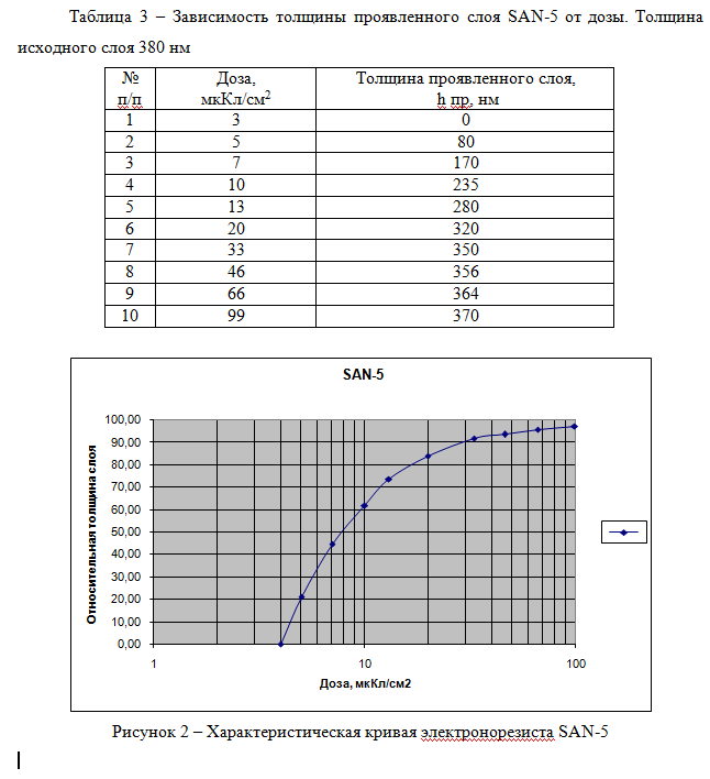
Sensitivity, Q0.5, electronic resistor - 8 µCl/cm2, gamma contrast - 2.2, working dose 20 µCl/cm2 (20 keV).
The process of pattern formation in a SAN layer:
Application on a centrifuge-30 with (application rate is determined by the application curve);
Drying I - 100°C, 2 min., hot plate, or thermal cabinet, 80-90°C, 20 min;
Exposure - 15-30 µCl/cm2 at 20 kV;
Appearance in SAN-D for 10 s (spray);
Flushing - propanol-2 - 12-20 s (spray);
Drying II - 100°C, 2 min., hot plate, or thermal cabinet, 80-90°C, 20 min;
Cleaning and removal - O2 plasma.